Congratulations to the grade 12 class that built these. Excellent work.
Here are the instructions I gave to the class:
INSTRUCTIONS
STEP 1
Manufacture
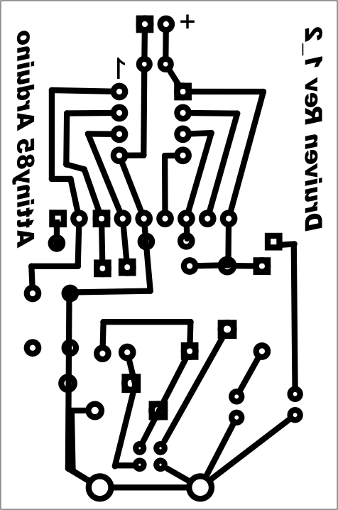
the circuit board using the trace layout given following the
classroom procedure. You may want to add 1/8 inch holes in each
corner so that your board can be mounted using 4/40 screws at a later
date.
STEP 2
Familiarize
yourself with the schematic diagram and parts placement.
Identify
the following parts:
- USB signal
- Power
- Reset
- i/o
STEP 3
Place
the components and solder them in place in the following order. Clip
the excess leads after each set of components is soldered.
- Capacitors
- 8 pin socket
- 1.5kΩ resistors
- 1N4148
- 22Ω resistors
- 3.6V zener diodes
- LEDs
- reset pushbutton
- 9 pin header
- USB socket
STEP 4
Use a
multimeter to check for shorts between traces. Notice that the USB
power and signal traces are very close together and a USB short could
affect your computer. If there are no shorts connect your Atiny85
Arduino via USB to a laptop for a moment. The green power LED should
glow (and hopefully nothing else will happen).
STEP 5
Unzip
the Digispark Arduino IDE and locate the directory in the installs
directory on a school laptop.
STEP 6
Use the
InstallDriver utility inside
/DigisparkArduino-Win32/DigisparkWindowsDriver to install the driver.
STEP 7
Run the
Arduino IDE inside of
/DigisparkArduino-Win32/Digispark-Arduino-1.0.4/
- Do not connect your Atiny85 Arduino to the computer yet.
- Under Tools choose Board and choose Digispark (Tiny Core).
- Under Tools choose Programmer and choose Digispark.
- Under File choose Examples and choose Digispark_Examples and choose Start.
- Click the upload button and watch the message area at the bottom of the IDE.
- Plug in your Atiny85 Arduino when the “Plug in device now . . .” message appears. Pin1 (sometimes called PB1) is pin 6 on the chip. Your built in red LED is connected to this pin. The program should cycle the LED on and off at 1 Hz.
Handy
Reference Chart
| pin | Pin | Analog |
| 1 | Reset | |
| 2 | 3 | Input 3 |
| 3 | 4 | Input 2 |
| 4 | Gnd | |
| 5 | 0 | PWM,AREF,MOSI |
| 6 | 1 | PWM, MISO |
| 7 | 2 | Input 1, SCK |
| 8 | VCC |
Here is a pdf file containing a sheet of 16 pcb layouts.


Would it be possible to share the source files and PCB for this project?
ReplyDeleteRegards
We've started on making up proper source files this month. The original source file was done in Fritzing, imported and improved in Corel Draw.
ReplyDelete